Microelectronics Manufacturer
Facility
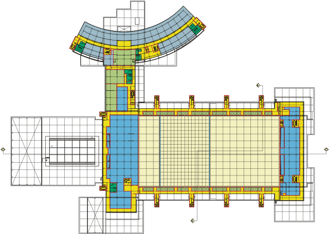
Semiconductor manufacturing facility 1, new 300mm manufacturing plant including 8,000 m² cleanroom and 1,000 m² of analytical labs.
Semiconductor manufacturing facility 2 various expansion and upgrade projects for semiconductor manufacturing
1998 – 2006
Role
Senior Architect for CH2M
Project Description
The planning and detail design of the ISO 5 manufacturing cleanroom plus various clean support areas including laboratories. The projects varied in size from 500 m² to 8,000 m².
Scope
The design of analytical laboratories with critical environments including metrology and characterisation laboratories. These housed a range of equipment including: Scanning Electron Microscopes and Transmission Electron Microscopes
Contact us
This site is protected by reCAPTCHA and the Google Privacy Policy and Terms of Service apply.

